
Sensicomm LLC - DSP design services.
Algorithms, software and hardware for sensors, signal processing, and communications.Home About Contact Publications Projects Downloads Sitemap Blog
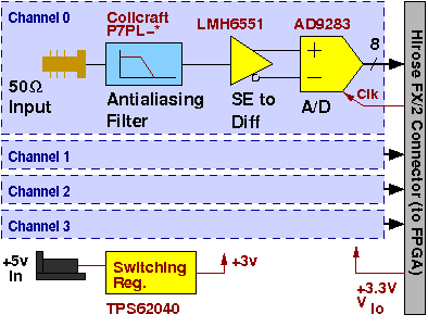
I plan to use the Spartan-III FPGA for various DSP functions, so I decided to build an A/D board for testing. The board includes (for each channel):
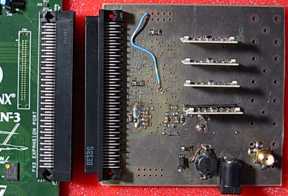
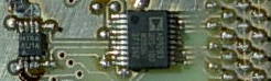 The board is double-sided, and was laid out using Kicad. The A/D and buffer amp are placed on the
bottom side, which allows short and direct PCB traces to the connector pins (photo to left). All
bypass capacitors and other passives are on the top side of the PCB.
The board is double-sided, and was laid out using Kicad. The A/D and buffer amp are placed on the
bottom side, which allows short and direct PCB traces to the connector pins (photo to left). All
bypass capacitors and other passives are on the top side of the PCB.
![]() Currently (Dec 2008), one channel is fully populated for testing. Power is being obtained
directly from the FPGA board rather from the on-board regulator. The A/D and buffer are
working as expected. For this test plot, the A/D is being clocked at 50MHz, and the input
signal is being generated using a 4-bit DAC constructed from an R-2R resistor network
connected to an available FPGA output port. The DAC is being driven by a counter, so
the output is a sawtooth waveform (linear ramp from min to max, followed by an
abrupt drop back to min).
Currently (Dec 2008), one channel is fully populated for testing. Power is being obtained
directly from the FPGA board rather from the on-board regulator. The A/D and buffer are
working as expected. For this test plot, the A/D is being clocked at 50MHz, and the input
signal is being generated using a 4-bit DAC constructed from an R-2R resistor network
connected to an available FPGA output port. The DAC is being driven by a counter, so
the output is a sawtooth waveform (linear ramp from min to max, followed by an
abrupt drop back to min).
(Mar. 2009) The FPGA code routes the 50MHz XTAL oscillator signal to the A/D board for use as a sampling clock. I tried using the Digital Clock Multiplier (DCM) in the FPGA to double the clock rate to 100MHz, but operation in that mode was not reliable. Sometimes the captured signal looks clean, but other times I see sharp jumps in the signal. The problem appears to be jitter in the DCM output signal, so that the A/D output bits are not being consistently sampled at the correct time. Next step is to try a 100 MHz oscillator, to see if a clean clock signal works at this speed.
(Apr. 2009) The A/D is now sampling cleanly at 100MHz. The problem was in adjusting the
timing relationship between the sampling clock and the latches in the FPGA.
It works now that the attributes CLOCK_SIGNAL, IOB, and
IBUF_DELAY_VALUE are set properly.
I now have two versions of the VHDL code. Both versions capture the A/D outputs and sequentially store them in one of the on-chip 16 kbit dual port RAM modules that are an integral feature of the Xilinx Spartan FPGA's. The RAM is configured as 2048x8, so 2048 contiguous samples are saved per A/D.
The original version of the FPGA code runs on the Spartan 3AN development board, and it reads the captured samples from the dual port RAM and displays them using the VGA display port. My VGA control logic displays a 500 or so sample segment of the signal. It reads the segment once for every scan line, and lights the appropriate pixels to produce a plot of the waveform. The waveform plot above was obtained by photographing a VGA output display.
The second version of the FPGA code runs on the Nexys 2 board from Digilent. It uses the onboard Cypress USB interface to upload the captured samples to a PC.
Why two versions, you may ask? Well, I found that the USB interface on the 3AN board is undocumented, and does not seem to support fast data transfers to the host. So, I would need to add an external USB interface to do uploads, while the Nexys board requires only a software download to support data transfers. A related webpage digilent_nexys_usb.shtml Talks in more detail about USB interfacing.
My long-term plan is to merge the two versions into a single package that supports both VGA display and USB uploading, and that works on the Nexys board.
For initial testing, I wrote a package to interface with Octave ( www.gnu.org/software/octave ). It uses a loadable module (MEX file) to talk to the Digilent board, and supports commands to trigger a capture of 2048 samples and to upload those samples to the host.
The Octave MEX files are approximately source code compatible with Matlab MEX files, so it should easy to port the code to Matlab. (Future project).
Based on the parts cost, I estimate the board could be produced in small quantities for about $150 for a one-channel version, plus about $60 for each additional channel. I'm not planning to do this as volume production, but I could make a few more if anybody's interested. If so, send me an email (contact info link at top of page).